







 Global
  United States
 Japan
Japan 






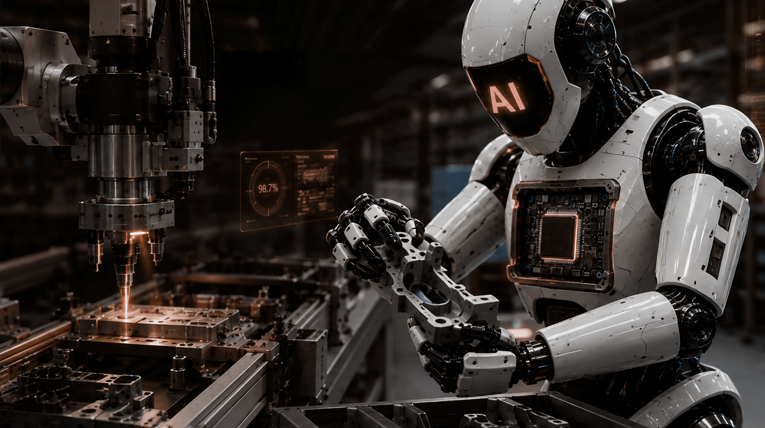
For most of the last decade, “AI hardware” meant one thing: bigger GPUs, bigger data centers, bigger context windows. That story worked as long as intelligence lived inside a browser tab. It stops working the moment intelligence has to open a door, pick up an irregularly shaped part off a conveyor or catch itself after a stumble on uneven ground.
That’s the shift the industry now calls Physical AI. AI systems that perceive, reason and act inside real, unstructured, physically consequential environments, on hardware that has to work in real time, on a power and thermal budget, without a cloud connection to lean on when the network hiccups. A humanoid robot doesn’t get to wait 400ms for a round trip to an inference server before deciding whether the object in its gripper is slipping. A mobile robot navigating a warehouse aisle doesn’t get to retry a control loop it missed. In Physical AI, latency isn’t a UX metric – it’s a safety spec.
This piece is about the hardware reality underneath that shift: what actually has to sit inside a modern robot’s chassis, why the “just add a bigger GPU” playbook from the LLM world doesn’t transfer cleanly, and why the companies that can actually engineer and manufacture this hardware – not just design the chip inside it – are becoming the real bottleneck, and the real opportunity, in Physical AI.
Table of Contents
Why Physical AI breaks the datacenter playbook
A cloud AI system is optimized around one variable: throughput per dollar. A robot is optimized around a much messier set of constraints stacked on top of each other:
● Real-time determinism. A robot’s control loop, the layer that keeps a joint from overshooting, a gripper from crushing, a chassis from tipping – typically has to close in the sub-millisecond to low-millisecond range, with jitter bounded tightly enough that a missed cycle doesn’t become a safety incident. General-purpose GPU compute, tuned for batch throughput, is a poor fit for this layer on its own.
● Multi-modal perception under power and thermal limits. Cameras, depth sensors, LiDAR, IMUs, force-torque sensors and increasingly tactile skin sensors all have to be fused into a coherent world model, continuously, on a battery-powered platform that can’t carry a server rack’s worth of cooling.
● Heterogeneous workloads on one board. A single robot brain typically needs a CPU for orchestration and safety-critical logic, a GPU or NPU for perception and learned policies and often an FPGA or adaptive SoC fabric for deterministic sensor I/O and functional-safety interlocks – three very different compute paradigms that all have to share power, board space and a thermal envelope.
● The sim-to-real gap. Policies trained in simulation routinely degrade when deployed on physical hardware, because simulated friction, contact dynamics and sensor noise are only approximations. Closing that gap increasingly depends on how much compute the robot has on-board to adapt and correct in the field, not just how good the training run was.
● Vendor lock-in risk. Robotics companies building multi-year product lines are wary of tying an entire platform to a single closed compute stack; the industry is visibly moving toward open software ecosystems that let the same policy stack run across silicon generations.
None of this is solved by scaling a data-center GPU down. It requires purpose-built silicon that treats CPU, GPU/NPU and adaptive logic as first-class, co-designed citizens on the same chip or module and it requires that silicon to actually make it into a manufacturable, certifiable, mass-produced robot, which is a very different problem from shipping a chip.
The three-layer stack of a modern robot brain
Strip away the marketing language and most Physical AI platforms converge on a similar architecture:
1. Sensing and safety layer: deterministic, low-latency logic (often FPGA/adaptive SoC based) that handles sensor fusion, functional-safety interlocks and hard real-time control, independent of whatever the AI stack above it is doing.
2. Perception and reasoning layer: CPU + GPU/NPU compute running the vision, language and decision-making models: object detection, scene understanding and increasingly Vision-Language-Action (VLA) models that map raw sensor input directly to robot actions.
3. Systems and manufacturing layer: the physical realization: board design, thermal engineering, ruggedization, EMI compliance, camera and connector integration and the supply chain and manufacturing discipline needed to take a reference design from a handful of prototypes to thousands of units a quarter.
Layers 1 and 2 get most of the press. Layer 3 is where most robotics programs actually die — and it’s the layer this piece is really about.
Spotlight: The engineering and manufacturing bridge for Physical AI
A reference design is not a product. Between “the chip works on a dev kit” and “a fleet of 10,000 robots ships reliably to customers” sits an enormous amount of unglamorous engineering: multi-layer board design that keeps a CPU, GPU/NPU and adaptive SoC thermally sane in a compact chassis; camera and sensor integration tuned for real-world lighting and vibration, not a lab bench; EMI/EMC and safety compliance; and a manufacturing line that can hold tolerance across tens of thousands of units without a single silent defect propagating into a safety-critical robot.
This is the layer where VVDN Technologies has built its position – not as a chip designer, but as the engineering and manufacturing bridge that takes heterogeneous compute platforms and turns them into deployable, certifiable robotics hardware. That work spans the full arc of what Layer 3 actually demands:
- End-to-end product engineering, from board design and firmware through mechanical and thermal engineering, so that a reference platform’s CPU/GPU/NPU/adaptive-SoC mix survives contact with a real chassis, real vibration and a real duty cycle instead of a lab bench.
- Vision and sensor-fusion reference platforms purpose-built for the perception layer of Physical AI — camera, depth, LiDAR and IMU integration tuned for the lighting, EMI and ruggedization conditions robots actually operate in.
- Manufacturing at scale, using VVDN’s own PCB assembly, product assembly and testing/validation/certification lines to close the gap between a handful of prototypes and thousands of units a quarter without quality drift.
- Physical AI inside its own factories. Notably, VVDN has been applying the very technology category it builds hardware for back into its own operations — embedding real-time, AI-driven vision systems into its robotic assembly cells to catch component-placement variances on high-density PCB and device assembly lines, including some of the same “odd-form” and SMT processes that produce boards destined for other companies’ robots. A manufacturing partner that is also using Physical AI to build is closer to the operational reality of what it takes to make Physical AI hardware reliable at volume — that’s not a marketing line, it’s a difference you can audit on the factory floor.
For robotics and Physical AI companies weighing the choice between building an in-house hardware team from scratch and partnering with an established ODM/engineering house, this combination – deep experience with edge AI and vision reference designs on modern heterogeneous silicon, plus in-house Physical AI-enabled manufacturing lines – is exactly the profile that shortens the path from prototype to a certifiable, mass-producible next-generation robot. It’s also why the manufacturing and systems-integration layer, not the chip alone, is becoming the real competitive moat in this industry.
The underlying silicon: adaptive-compute building blocks
None of the engineering above happens in a vacuum — it sits on top of silicon, and the industry’s compute options for Physical AI have gotten more open in the last year. AMD is one example worth a brief mention: its Kria AI System-on-Modules, the Ryzen AI Embedded X100 series (pairing “Zen 5” CPU cores with an RDNA 3.5 GPU and a dedicated NPU in one embedded part), and an open ROCm-based software stack are aimed specifically at collapsing what used to be three separate chips – real-time control, AI acceleration and a closed SDK – into fewer, more open building blocks.
Where this is heading
A few trends worth watching:
● VLA models are moving from research demos to production stacks. Vision-Language-Action models, which map camera and sensor input directly to robot motor commands – are the clearest sign that “AI for robots” and “AI for chat” are diverging architecturally and they demand tight co-design between the model and the silicon running it.
● Openness is becoming a purchasing criterion, not a philosophy. Robotics companies building multi-year hardware roadmaps are explicitly avoiding single-vendor lock-in on both silicon and software, favoring open compute ecosystems they can port policies across.
● Sim-to-real remains the central open problem. Domain randomization, better physics engines and synthetic data generation are narrowing the gap between simulated training and real-world reliability. However, it’s still the field’s hardest unsolved engineering question – and it’s as much a hardware/compute-budget problem as an algorithms one.
● The manufacturing layer is becoming a competitive moat. As more silicon vendors open up robotics-grade compute, the differentiator shifts downstream – to who can actually engineer, integrate, certify and manufacture that compute into a robot that survives contact with the real world.
Physical AI’s next breakthroughs won’t only come from a bigger model or an open chip. They’ll come from engineering partners like VVDN, who know how to turn heterogeneous silicon into a real, certifiable, manufacturable fleet – the unglamorous middle layer where Physical AI actually gets built.