


The article provides an overview of the typical semiconductor chip development process, the difference between pre-silicon verification and post-silicon validation, tools used in SoC / FPGA / ASIC development, emerging trends in semiconductor design and manufacturing along with VVDN expertise in the space of semiconductor design and engineering.
Table of Contents
Typical Development Process of Chip
The chip development process, also known as semiconductor or integrated circuit (IC) development, involves designing and manufacturing electronic chips that power a wide range of devices, from simple microcontrollers to advanced processors. Here’s an overview of the typical chip development process:
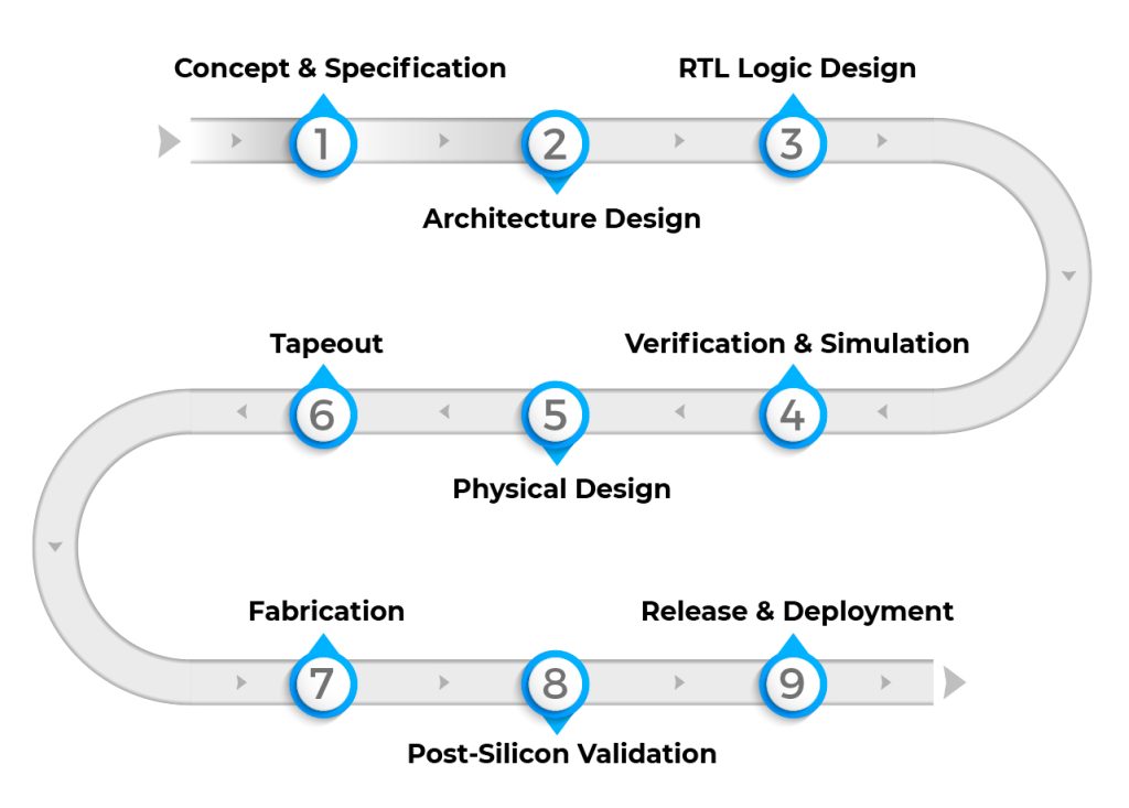
Concept and Specification:
The chip development process begins with defining the purpose of the chip, its intended functionality, and the target application. Engineers and designers collaborate to create a chip specification, outlining its key features, physical design, performance requirements, power consumption, cost, power, and other essential characteristics.
Architecture Design:
Based on the chip specifications, a high-level architectural design is developed that outlines the major functional blocks and their interconnections. This stage involves selecting appropriate technologies and methodologies to achieve the desired performance. The interfaces and protocols within the chips are also defined in this stage. The results of this stage serve as the foundation of subsequent stages, ensuring the development of an efficient chip with optimum performance.
RTL Logic Design:
The term RTL refers to Register Transfer Level. The objective of digital design is to convert the architectural concept into a behavioral model representing the chip. The logic design phase focuses on creating detailed circuit schematics for each functional block in the chip’s architecture. Hardware description languages (HDLs) like Verilog or VHDL are commonly used to represent the logic and behavior of the circuits. The RTL design specifies how the chip should function in terms of logical operations and data flow between memory blocks.
Verification and Simulation:
Before physically implementing the chip, extensive verification and simulation are conducted to ensure that the design functions correctly and meets the specifications. This involves running various tests and simulations to identify and resolve potential design flaws and bugs. Any design issues found at the verification stage are sent back to the digital design team for corrections until they are fixed.
Physical Design:
The physical design stage involves transforming the logical representation of the chip into a physical layout. The physical design of the chip can be broken down into multiple steps (illustrated below).
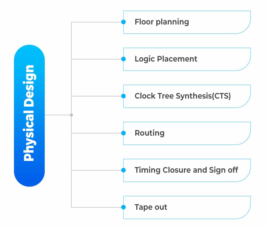
- Floorplanning: The process starts with floorplanning, where transistors, interconnects, and other components are placed on the chip’s silicon die with the help of Electronic Design Automation (EDA) software.
- Placement: Next, comes placement where all the standard cells in the design are placed and assigned a legal location. A number of optimizations and timing-driven placement algorithms are performed to optimize placements, meet timing constraints and minimize signal delays.
- Clock Tree Synthesis: Clock tree synthesis (CTS) is the stage after placement to make sure that the clock signals are distributed uniformly to all the sequential elements or flops. The objective of this stage is to create a good-quality clock network to meet the timing requirements for the design.
- Routing: Routing is connecting the various blocks in the chips with one another through metal traces. Routing ensures proper electrical connections while optimizing power integrity and signal integrity (PI/ SI).
- Timing Closure and Signoff: After routing, comes the timing closure and sign-off stage, a crucial step in the physical design. It analyzes the performance and functionality of the design by ensuring that all paths meet the timing requirements.
- Tape Out: It is the final stage where the physical design is completely verified, and the design data in graphic data system (GDS II) format is sent to the semiconductor foundry for fabrication.
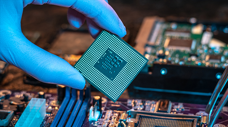
Fabrication:
Once the physical design is complete, the chip goes into the manufacturing phase. The chip design is sent to a semiconductor foundry, where it undergoes photolithography, etching, doping, and other processes to create the physical chip.
Post-Silicon Validation:
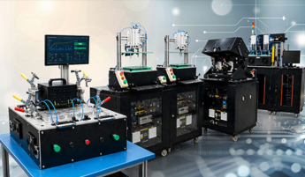
The escaped bugs during the pre-silicon verification stage are captured in the post-silicon validation stage. The prototypes of the chips received from the foundry are tested on reference/ evaluation boards for all functional correctness in a lab setup. The validation checks include many things apart from functional correctness such as compliance with power and performance for targeted use cases, thermal changes, electrical noise margins tolerance, and so on, The tests are performed on the real chips so it runs at the real system speed (in the range of GHz), so this is fast as compared to the pre-silicon verification stage. The overall goal of post-silicon validation is to make sure the Silicon/ ASIC/ SoC/ FPGA are qualified and ready to deploy.
Release and Deployment:
Once the chips pass all testing and quality assurance processes, they are released for integration into various electronic devices or systems.
Post-Release Support:
Manufacturers also provide ongoing support and updates, addressing any issues or improvements that may arise during the chip’s lifecycle.
Tools Used in SoC/ FPGA/ ASIC Development
System-on-Chip (SoC), Field-Programmable Gate Array (FPGA), and Application-Specific Integrated Circuit (ASIC) development involve a wide range of tools that help with designing, verifying, and implementing complex integrated circuits. Hardware Description Language (HDL) Editors and Integrated Development Environments (IDEs) enable efficient code writing and simulation. Logic Synthesis, Place and Route, and Static Timing Analysis (STA) tools optimize the design process, ensuring optimal performance. Verification and Debugging tools facilitate rigorous testing and troubleshooting of a particular chip that is in the design phase. Additionally, High-Level Synthesis (HLS) and Emulation platforms streamline development, while Power Analysis and Formal Verification tools further enhance efficiency. Many leading companies, such as Cadence, Xilinx/AMD, Intel/Altera, Synopsys, and Mentor, are providing tools for RTL, logic synthesis, place, and route, static timing analysis, physical verification, DFT, simulation, power analysis, and more. With these tools, the journey from concept to production becomes a seamless and transformative experience.
Emerging Trends in Semiconductor Development
The latest trends in semiconductor or chip development are driven by the need for more efficient and specialized processors that can be used in targeted applications. Some of the technologies driving the trends in semiconductor development are 5G, the Internet of Things (IoT), Autonomous vehicles, and Edge Computing. Chip developers are also adopting new technologies in chip development, such as Heterogeneous integration and Artificial intelligence, to develop chips with faster performance. Semiconductor technologies, like 7nm, 5nm, or beyond, are also unlocking greater performance and power efficiency. All of these collectively promise a future of a more connected and intelligent world.
How Does VVDN Help Chip Manufacturers in Semiconductor Design and Engineering?
The chip development process is complex and can take several months to years, depending on the complexity of the chip and the manufacturing technologies involved. VVDN offers a wide range of semiconductor engineering services to global chip manufacturers. Our specialization lies in helping semiconductor companies accelerate the development of their next-gen products/solutions. Our team of skilled engineers has extensive experience in ASIC/SoC/FPGA development, RTL design, physical design, pre-silicon verification, post-silicon validation, board bring-up, and reference hardware and firmware development.
Please feel free to reach out to us at info@vvdntech.com for further insights into our end-to-end semiconductor engineering capabilities and explore collaboration opportunities to accelerate your solution launch to the market.